How MIP Bridges the Gap from Mini to Micro LED Direct Display
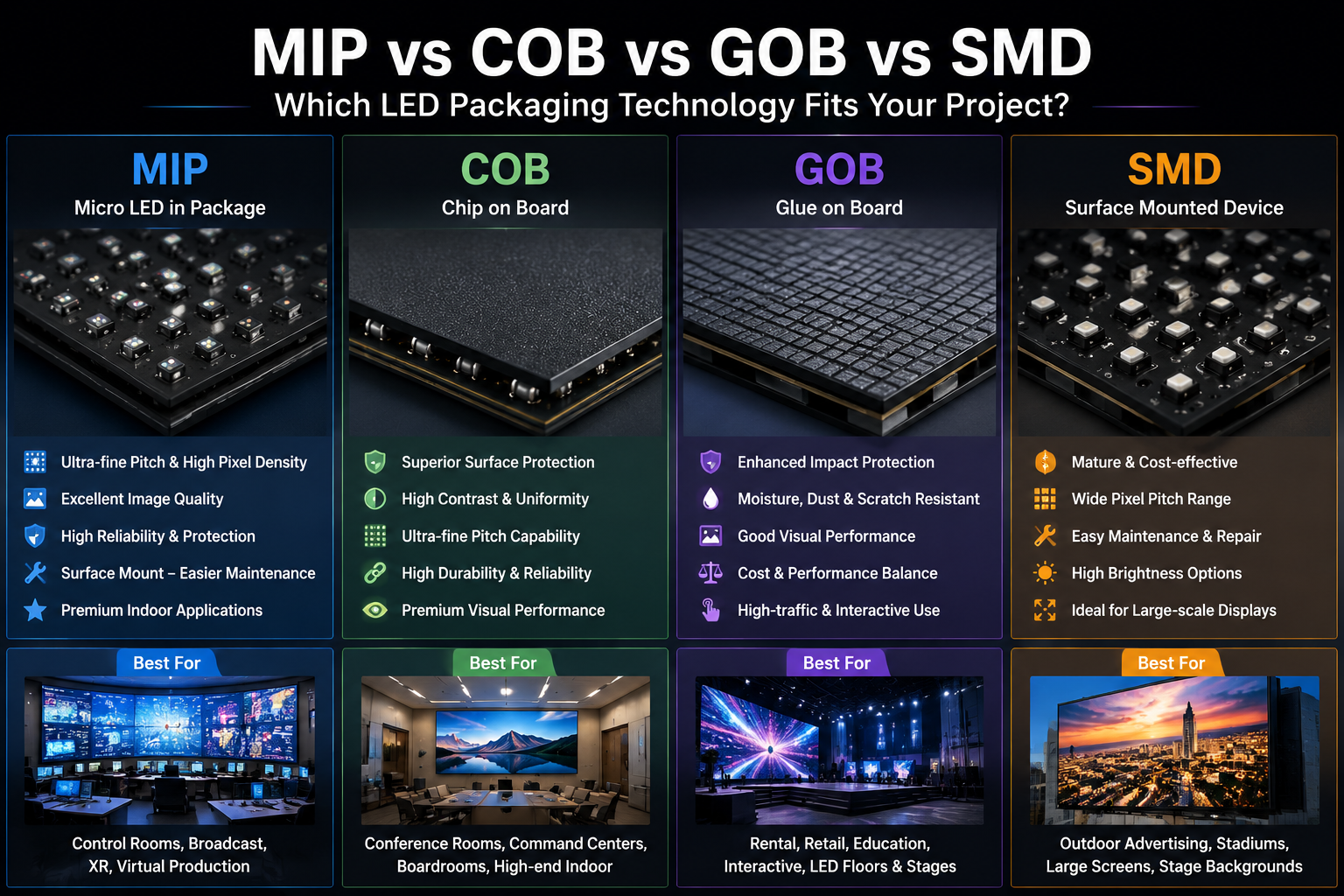
In the field of LED displays, packaging technology has evolved from early DIP, SMD, and IMD to COB, and now to the highly anticipated MIP (Mini/Micro LED in Package). This evolutionary curve is driving the direct-display industry toward higher resolutions, superior reliability, and lower power consumption.
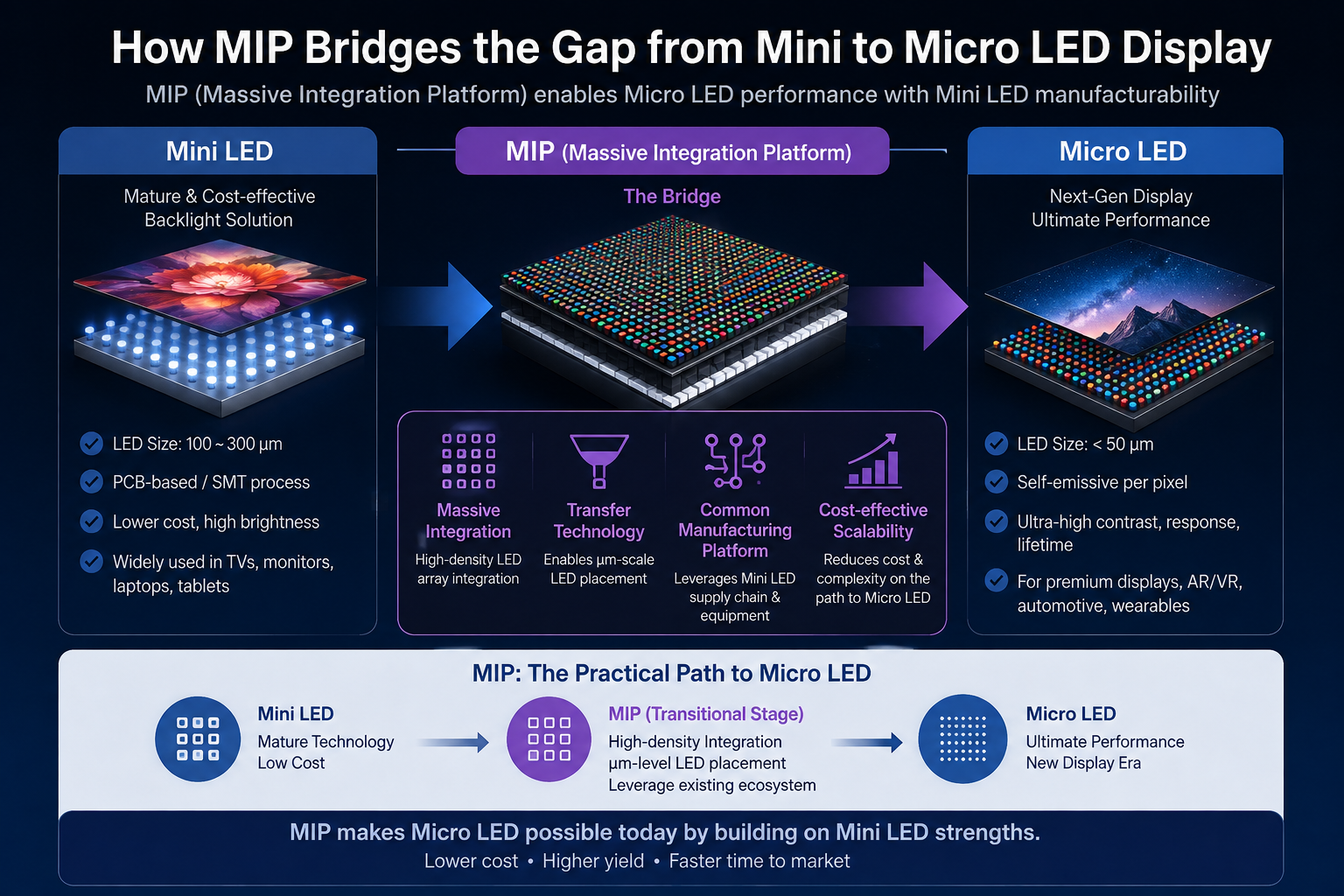
As Mini/Micro LEDs rapidly penetrate the market, MIP is widely regarded as the critical bridging technology connecting the Mini era to the Micro era.
However, many industry observers still confuse MIP with SMD and IMD. What are the structural differences between them? And what defines a true MIP implementation?
SMD: The Origin of the Surface-Mount Era
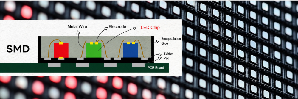
SMD (Surface Mount Device) was the earliest mainstream packaging form in the LED industry. Its core feature involves packaging three discrete (Red, Green, Blue) LEDs into a single lamp bead via face-up/vertical die attachment (where Red uses a vertical structure requiring one wire bond, while Blue and Green use face-up structures requiring two wire bonds). These lamp beads are subsequently surface-mounted onto a PCB board.
As pixel pitch continues to shrink, the limitations of SMD have become increasingly prominent:
Pixel Pitch Bottleneck: Large individual lamp bead sizes make achieving a fine pitch below P0.9 extremely difficult.
Inconsistent Optical Performance: Structural disparities across the three chips create micro-variations in height and optical axis deviation, leading to color shift and non-uniform brightness.
Lower Luminous Efficiency: Face-up/vertical structures yield smaller light-emitting areas (significantly shadowed by bond pads and gold wires), resulting in lower brightness compared to flip-chip alternatives at equivalent die sizes.
IMD: The Transition from Single Lamp to Multi-Pixel Integration
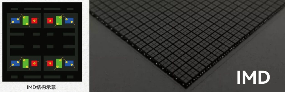
To address pixel pitch miniaturization, IMD (Integrated Matrix Device) emerged as an "n-in-1" architecture. It consolidates two or more RGB pixels into a single package body. The most commercially mature form is "4-in-1" (integrating 4 pixels into one package).
IMD balances the repairability of SMD with the high integration density of COB, serving as a widely adopted solution for early fine-pitch displays (P0.9–P0.6). Nevertheless, IMD essentially retains the core nature of "mounting lamp beads," involving complex packaging steps and limited automation. As pixel pitches approach sub-P0.6 levels, packaging precision and mounting efficiency bottlenecks re-emerge.
Furthermore, because the module pitch is fixed during the initial bead packaging stage, IMD offers limited manufacturing flexibility across multi-model or custom product lines.
MIP: The Shift from "Mounted Bead" to "Chip-Level Package"
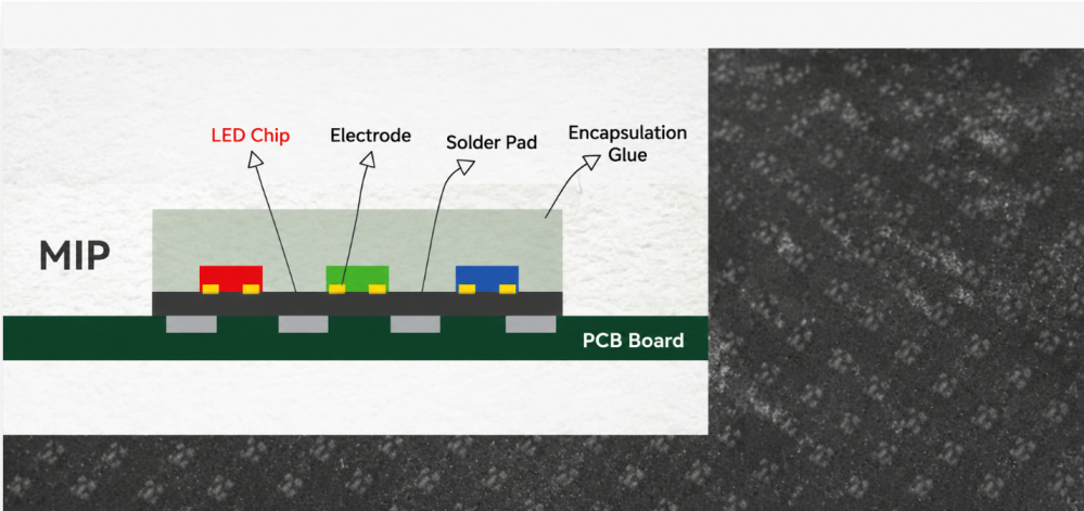
MIP (Mini/Micro LED in Package) shifts the paradigm: Mini/Micro LED chips are first flip-chip mounted into an intermediate package body to form an independent, stable light-emitting unit, before undergoing module-level integration or mounting.
The primary distinction between MIP and traditional SMD/IMD lies in the shift from a "lamp bead" focus to a "chip package body" focus. In simple terms: SMD and IMD mount pre-made lamp beads, whereas MIP packages bare chips directly into carrier units.
Structurally, MIP uses a wire-bondless flip chip COB LED display structure and die-bonding architecture. Eliminating wire bonding enables a far more compact footprint and superior reliability.
For downstream module and display manufacturers, MIP offers dual benefits: it works seamlessly with existing COB process equipment while enabling technical upgrades and capacity reuse. This lowers adoption barriers and avoids the steep supply chain costs associated with direct Micro LED deployment. Additionally, the package structure provides structural protection and reliability for the micro-chips.
This transition delivers four major advantages:
Ultra-Compact Package Architecture: Supports ultra-fine pixel pitches of P0.4 and below.
Enhanced Reliability: Chips are stress-protected by the package, significantly improving physical durability.
Broad Supply-Chain Compatibility: Downstream manufacturers can leverage existing equipment and workflows to minimize adoption thresholds.
Optimized Optical Consistency: Individual MIP units can be physically mixed and sorted by color/brightness before surface mounting, yielding superior display uniformity.
Consequently, MIP represents not only a packaging upgrade, but a vital intermediate layer bridging current Mini LED infrastructure with future Micro LED displays.
Given that monolithic Micro LED solutions (such as COG) still face yield and cost hurdles during mass transfer, advancing MIP packaging (via sapphire LLO, mass transfer, and RDL) shrinks bead sizes down to 0202 or 0101. This enables ultra-fine pitch modules (sub-P0.6)—such as high-density P0.9 COB LED display panels—that remain challenging for direct COB processes.
Currently, MIP packaging is categorized into Mini-level MIP and Micro-level MIP, differentiated by chip size and substrate-stripping processes.
Mini-level MIP (Mini LED in Package)
Mini-level MIP typically uses flip-chip Mini LEDs ranging from 100 µm to 300 µm that retain their sapphire substrate. These are assembled via die-bonding into MIP packages (commonly 0404 or 0606 footprints).
The primary bottleneck lies in front-end packaging: efficiently and reliably sealing Mini chips into MIP bodies. Because transfer efficiency and yield dictate overall cost, front-end packaging accounts for the majority of Mini-level MIP expenditure. According to TrendForce analysis, the MIP package body accounts for up to 31% of total costs in a 0404 MIP display module, whereas PCB and back-end die-bonding costs are reduced.
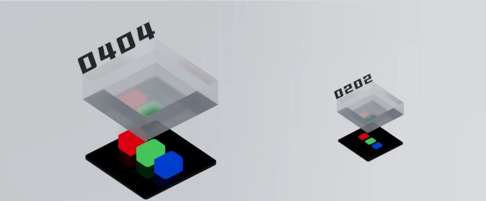
Key advantages of Mini-level MIP include:
High Packaging Efficiency: Downstream module makers transfer all three RGB Mini LED chips simultaneously during a single die-bonding step, tripling packaging efficiency.
Relaxed Tolerance & High Yield: Package dimensions, pin spacing, and gap distances are considerably larger than bare flip-chip Mini LEDs. This lowers requirements for PCB density and placement precision, boosting overall yields.
Optimized Optical Uniformity: MIP allows physical color mixing ("灯珠炒光" / physical binning) before placement, improving screen uniformity and reducing secondary module sorting steps.
As chip and packaging manufacturers mature their production capacity and solve process bottlenecks, the cost of Mini-level MIP is projected to decline further, providing a highly cost-effective Mini LED direct-display path.
Micro-level MIP (Micro LED in Package)
When LED chip sizes shrink below 100 µm (Micro level), mounting them directly onto display modules creates severe challenges in electrical interconnections, yield loss, and chip reliability. Furthermore, traditional wafer grinding/thinning on sapphire-backed sub-100 µm chips reaches a physical bottleneck—frequently causing wafer cracking and dropping yields below 50%. This necessitates Laser Lift-Off (LLO) technology to strip the sapphire substrate.
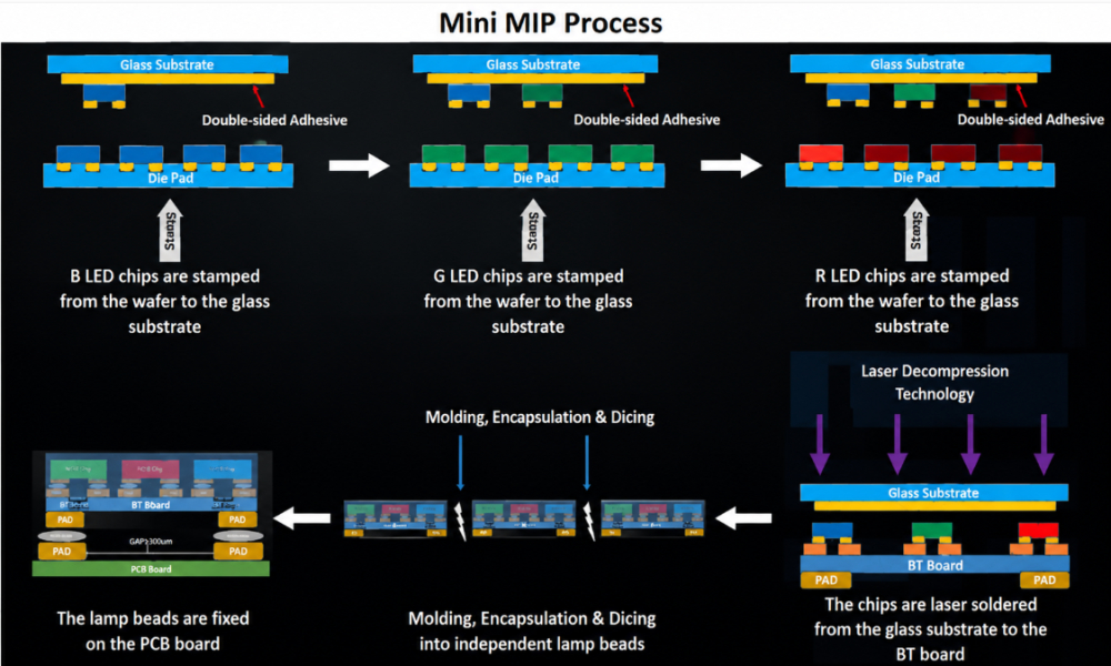
Micro-level MIP utilizes ultra-small RGB Micro LED chips (<100 µm) with stripped sapphire substrates, achieving true chip-level packaging for every next-generation Micro LED display.
Structurally, Micro-level MIP employs a flip-chip + die-bonding pre-packaging approach. Micro-scale chips are integrated into larger, structurally stable MIP package bodies via advanced packaging workflows (Sapphire LLO + Mass Transfer + RDL). This simplifies back-end module manufacturing while solving repair, yield, and line compatibility pain points.
The primary hurdle for Micro-level MIP lies in back-end chip processing: achieving efficient sapphire substrate stripping and overcoming mass transfer yield limits for Micro chips. Due to high bare-chip costs and complex processing, this technology remains in the yield-ramp phase prior to full mass market adoption.
Core advantages of Micro-level MIP include:
Superior Optical Performance: Post-LLO chip thickness drops below 10 µm. Reduced RGB chip areas and inter-chip spacing yield enhanced color mixing, eliminating off-axis color cast and blue/yellow lines.
Exceptional Contrast: Wire-free structures maximize the black matrix area around micro-scale chips, achieving ultra-high contrast ratios exceeding 10,000:1.
High Reliability: The substrate-free, wire-free design uses integrated pad and trace layouts to prevent silver migration and related failure modes.
Chip Cost Reduction Potential: Shrinking chip dimensions dramatically increases usable die count per wafer, offering long-term cost-reduction potential for Micro LED chips.
Simplified Module Assembly & Higher Yields: For module factories, the enlarged MIP footprint relaxes PCB substrate precision requirements, bypassing critical chip-to-panel manufacturing bottlenecks and increasing production throughput.
Equipment Compatibility: 0202 and 0303 MIP units can be mounted using standard COB surface-mount equipment, enabling asset re-use and smooth line upgrades.
Real-World Case Study: Micro-Level MIP in Commercial Applications
Micro-level MIP technology is rapidly transforming high-end commercial environments, offering ideal solutions for mission-critical installations such as a command center COB video wall or a premium boardroom COB LED screen.
Display Architecture: The module utilizes Micro LED chips with stripped sapphire substrates (<10 µm emitter thickness), improving luminous efficiency and operational stability.
Structural Design: Featuring a standardized 150 × 168.75 mm module design compatible with standard 600 mm cabinets, the layout provides mounting flexibility across diverse application scenarios while simplifying hardware upgrades.
As Micro LED fabrication and substrate stripping technologies continue to mature, Micro-level MIP is poised to become a decisive gateway to commercial Micro LED mass production.